|
The wavelength division multiplexing device connects multiple lasers, modulators, detectors, etc. on the chip, so that the transmission rate and processing rate of the on-chip data can be multiplied. The EPIC group systematically studied the wavelength division multiplexing/demultiplexer, and designed and fabricated an 8×8 cyclic arrayed waveguide grating device, which achieved a minimum loss of 2.4dB and crosstalk of -17.5dB~-25.1dB. The device performance has reached the international first-class level.
In the field of optical communication and optical interconnection, the wavelength division multiplexing technology has matured and widely applied. The wavelength division multiplexing/demultiplexer combines/demultiplexes multiple wavelengths so that different signals are transmitted and reprocessed in the same path. Arrayed waveguide gratings are a typical wavelength division multiplexing/demultiplexing device. It consists of a slab waveguide, an arrayed waveguide, and an input and output waveguide, as shown in Figure 1. The mechanism of action is that multiple wavelengths of optical signals enter the input slab waveguide region from the input waveguide, and are diffracted into a beam of light in the slab waveguide, which is almost uniformly coupled into the array waveguide port; after transmission through the array waveguide, due to different optical paths, For a certain wavelength of light wave, the output light phase at the end of the array waveguide is arranged in an equal sequence, and at the same time, the effective refractive indices of different wavelengths in the waveguide are different, resulting in different phase differences of the optical signals of each wavelength; In the output slab waveguide, these optical signals with different phase differences will interfere. According to the reflection characteristics of the Roland circle, the light waves of the same wavelength will be concentrated to a specific position of the small circle, that is, the port of the corresponding output waveguide. Therefore, the wavelength division can be realized by strictly calculating the length difference of the arrayed waveguide.
|
|
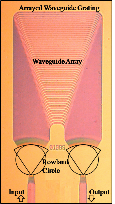 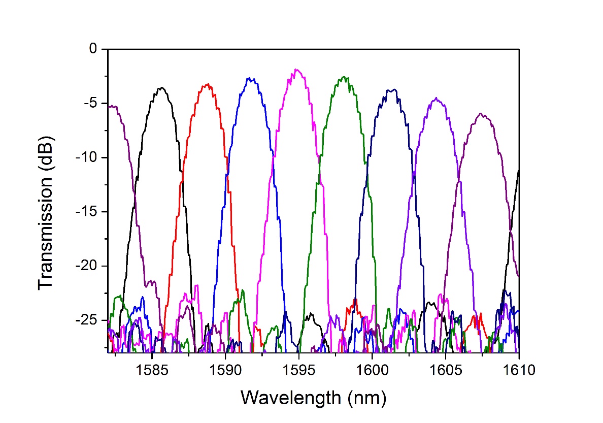
Figure 1 AWG schematic and test spectrum
|
|
At present, Ghent University, AIDI, PECST, A*Star, etc., domestic microsystems, Zhejiang University, and semiconductor institutes all report on SOI-based AWG. We have also carried out related research in this field. The research method is: using the transfer matrix method and the way of Finite Difference in Time Domain to simulate the structure of the arrayed waveguide grating; the arrayed waveguide grating device on SOI chip is fabricated by electron beam exposure and plasma inductive coupling etching, etc.
Figure 1 shows the AWG components designed and fabricated by the EPIC group, with the microscope view on the left and the 8-channel test curve on the right. We optimize the design of the arrayed waveguide grating in structure, and connect the slab waveguide and the single-mode waveguide with a fast-converging parabolic zonal conversion structure to reduce the coupling between adjacent channels to reduce the crosstalk and optimize the performance. We produced an 8-channel circulating AWG device with excellent performance in a simple single-layer etch process with 400 GHz channel spacing, 2.2 nm peak-width, minimum 2.4 dB loss, and -17.5 dB~-25.1 dB crosstalk. The device performance has reached the international first-class level. Related papers were published in the 2014 Optical Society of America Optics Express [1].
[1] Tong Ye, Yunfei Fu, Lei Qiao, and Tao Chu, “Low-crosstalk Si arrayed waveguide grating with parabolic tapers,” Opt. Express. 22(26), 31899–31906 (2014).
|
|